P-N Junction Diode: Essential Electronics Component for Circuit Design
P-N Junction Diode: A Cornerstone of Circuit Design
The P-N Junction Diode is an essential electronics component widely used in various electronic circuits. It serves as a fundamental building block in the world of electronics, enabling the flow of current in a specific direction while blocking it in the opposite direction. Comprising two regions — the P-type and N-type semiconductors — the P-N Junction Diode plays a crucial role in rectifying current, signal modulation, and ensuring the proper functioning of various electronic devices.
Objective:
To study Forward & Reverse Characteristics of PN Junction Diode.
Features:
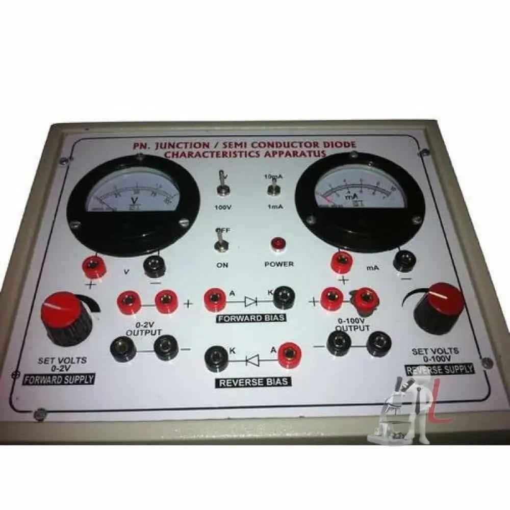
Instrument comprises of two DC Regulated Power Supplies 0-3VDC/150mA & 0-30 VDC/150mA, two dual range round meters for voltage & current measurement, PN Junction Diodes mounted behind the panel, connections of Supplies, Meters & Diodes brought out at 4 mm Sockets.
Accessories:
Set of Patch Chords, Instruction Manual
The P-N Junction Diode operates based on the principles of semiconductor physics. In a semiconductor material, impurities are intentionally added to create either a P-type or N-type region. The P-type region is formed by doping the semiconductor with elements that have fewer valence electrons (such as boron), resulting in 'holes' that act as positive charge carriers. Conversely, the N-type region is created by doping with elements that have more valence electrons (such as phosphorus), leading to an abundance of free electrons that act as negative charge carriers.
When these two differently doped regions are joined together to form a P-N junction, a depletion region is created at the junction interface. This region is characterized by a lack of charge carriers and acts as an insulator under certain conditions. When a forward voltage is applied across the P-N Junction Diode, it reduces the potential barrier of the depletion region, allowing current to flow through the diode. This property of conductance under forward bias and non-conductance under reverse bias is what makes the P-N Junction Diode an invaluable component in electronic circuit design.
The application of P-N Junction Diodes extends beyond simple rectification. In power supply circuits, they are commonly used as rectifiers to convert alternating current (AC) to direct current (DC). The use of a bridge rectifier circuit, which comprises four P-N Junction Diodes, is a widely adopted method of achieving full-wave rectification, providing a smoother output voltage suitable for powering electronic devices.
Moreover, the P-N Junction Diode also plays a significant role in signal processing. In radio frequency (RF) applications, they are often utilized in demodulator circuits to extract audio signals from modulated carrier waves. The superheterodyne receiver, popular in many electronics, employs P-N Junction Diodes to perform this function effectively.
Another vital application of P-N Junction Diodes is in the realm of light-emitting diodes (LEDs) and laser diodes. When a forward bias is applied, electrons recombine with holes in the P-N region, releasing energy in the form of photons — the basic principle behind LED operation. This technology has transformed lighting and display systems due to its energy efficiency and long lifespan.
P-N Junction Diodes also find applications in protection circuits. They are frequently used as flyback diodes in inductive load switching applications, where they prevent harmful voltage spikes caused by inductive kickback from damaging delicate electronic components, such as transistors or microcontrollers.
In conclusion, the P-N Junction Diode is an integral part of electronic circuit design, enabling diverse functions ranging from rectification to signal demodulation and light emission. Its unique characteristics and reliable performance make it indispensable for engineers and designers aiming to create efficient and effective electronic devices.
Original: $19.90
-70%$19.90
$5.97Product Information
Product Information
Shipping & Returns
Shipping & Returns
Description
P-N Junction Diode: A Cornerstone of Circuit Design
The P-N Junction Diode is an essential electronics component widely used in various electronic circuits. It serves as a fundamental building block in the world of electronics, enabling the flow of current in a specific direction while blocking it in the opposite direction. Comprising two regions — the P-type and N-type semiconductors — the P-N Junction Diode plays a crucial role in rectifying current, signal modulation, and ensuring the proper functioning of various electronic devices.
Objective:
To study Forward & Reverse Characteristics of PN Junction Diode.
Features:
Instrument comprises of two DC Regulated Power Supplies 0-3VDC/150mA & 0-30 VDC/150mA, two dual range round meters for voltage & current measurement, PN Junction Diodes mounted behind the panel, connections of Supplies, Meters & Diodes brought out at 4 mm Sockets.
Accessories:
Set of Patch Chords, Instruction Manual
The P-N Junction Diode operates based on the principles of semiconductor physics. In a semiconductor material, impurities are intentionally added to create either a P-type or N-type region. The P-type region is formed by doping the semiconductor with elements that have fewer valence electrons (such as boron), resulting in 'holes' that act as positive charge carriers. Conversely, the N-type region is created by doping with elements that have more valence electrons (such as phosphorus), leading to an abundance of free electrons that act as negative charge carriers.
When these two differently doped regions are joined together to form a P-N junction, a depletion region is created at the junction interface. This region is characterized by a lack of charge carriers and acts as an insulator under certain conditions. When a forward voltage is applied across the P-N Junction Diode, it reduces the potential barrier of the depletion region, allowing current to flow through the diode. This property of conductance under forward bias and non-conductance under reverse bias is what makes the P-N Junction Diode an invaluable component in electronic circuit design.
The application of P-N Junction Diodes extends beyond simple rectification. In power supply circuits, they are commonly used as rectifiers to convert alternating current (AC) to direct current (DC). The use of a bridge rectifier circuit, which comprises four P-N Junction Diodes, is a widely adopted method of achieving full-wave rectification, providing a smoother output voltage suitable for powering electronic devices.
Moreover, the P-N Junction Diode also plays a significant role in signal processing. In radio frequency (RF) applications, they are often utilized in demodulator circuits to extract audio signals from modulated carrier waves. The superheterodyne receiver, popular in many electronics, employs P-N Junction Diodes to perform this function effectively.
Another vital application of P-N Junction Diodes is in the realm of light-emitting diodes (LEDs) and laser diodes. When a forward bias is applied, electrons recombine with holes in the P-N region, releasing energy in the form of photons — the basic principle behind LED operation. This technology has transformed lighting and display systems due to its energy efficiency and long lifespan.
P-N Junction Diodes also find applications in protection circuits. They are frequently used as flyback diodes in inductive load switching applications, where they prevent harmful voltage spikes caused by inductive kickback from damaging delicate electronic components, such as transistors or microcontrollers.
In conclusion, the P-N Junction Diode is an integral part of electronic circuit design, enabling diverse functions ranging from rectification to signal demodulation and light emission. Its unique characteristics and reliable performance make it indispensable for engineers and designers aiming to create efficient and effective electronic devices.